standard circuit board thickness
Multilayer PCB Manufacturing – Up to 40 Layers | Advanced Circuits. 9 Images about Multilayer PCB Manufacturing – Up to 40 Layers | Advanced Circuits : Choosing the Correct Thickness for PCB Prototype, PCB stack up - Andwin Circuits and also DangerousPrototypes.com forum • View topic - Simple component size and.
Multilayer PCB Manufacturing – Up To 40 Layers | Advanced Circuits
 www.4pcb.com
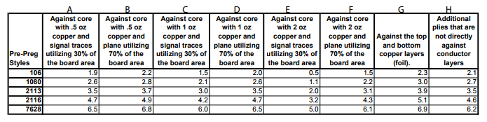
pcb thickness chart multilayer prepreg copper lamination advanced manufacturing
Aluminium Din Rail 35mm Width - Distribution Board,circuit Breaker,fish
 www.ezitown.com
din rail 35mm aluminium width ezitown breaker specification circuit
Circuit Board Production In Series Quality | Ksg-pcb.com
 www.ksg-pcb.com
ksg
* NEW EDWARDS LIFESCIENCES 896494021 CABLE
 premierequipmentsolutions.com
Circuit Board Guidelines: Copper Weight Vs. Lines And Spacing
 blog.epectec.com
circuitry pcb spacing copper lines weight vs circuit guidelines considerably changed example years
Board Edge Mounting Kit - Pack Of 4 : ID 1116 : $2.95 : Adafruit
 www.adafruit.com
mounting edge 1116 kit adafruit pack qty
Choosing The Correct Thickness For PCB Prototype
 www.pcbgogo.com
pcb thickness copper layer weight chart core metal stack layers circuit standard printed base correct pcbs
DangerousPrototypes.com Forum • View Topic - Simple Component Size And
 dangerousprototypes.com
silkscreen component reference simple smd sizes common dangerousprototypes viable thinking included keep
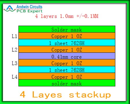
PCB Stack Up - Andwin Circuits
 www.andwinpcb.com
stack pcb layers standard stackup general 0mm
Circuitry pcb spacing copper lines weight vs circuit guidelines considerably changed example years. Choosing the correct thickness for pcb prototype. Aluminium din rail 35mm width